- 您现在的位置:买卖IC网 > Sheet目录2010 > MAX5216BGUA+T (Maxim Integrated Products)IC DAC 16BIT SPI/SRL 8UMAX
4
Maxim Integrated
14-/16-Bit, Low-Power, Buffered Output,
Rail-to-Rail DACs with SPI Interface
MAX5214/MAX5216
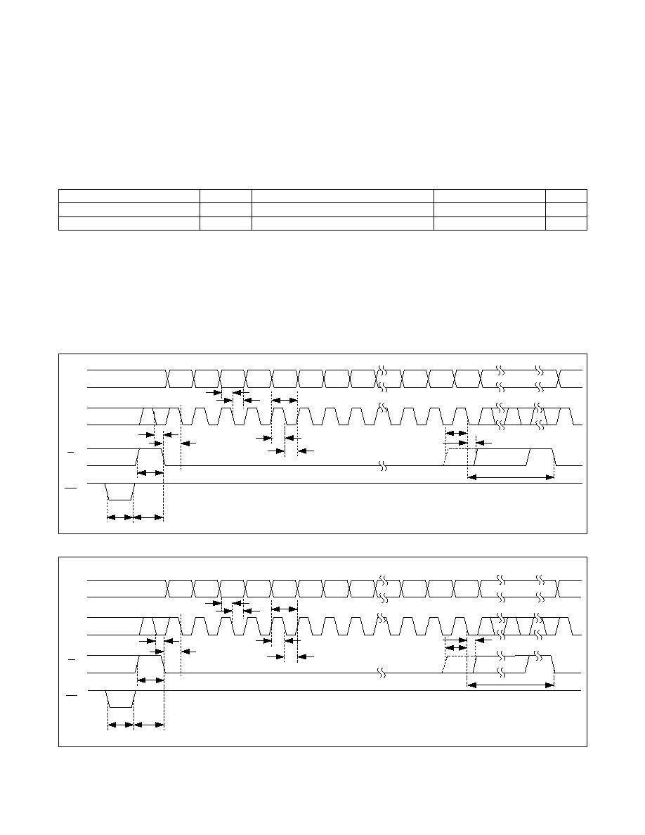
Figure 1. 16-Bit Serial-Interface Timing Diagram (MAX5214)
Figure 2. 24-Bit Serial-Interface Timing Diagram (MAX5216)
ELECTRICAL CHARACTERISTICS (continued)
(VDD = 2.7V to 5.5V, VREF = 2.5V to VDD, CL = 60pF, RL = 10kI, TA = -40NC to +105NC, unless otherwise noted. Typical values are
at TA = +25NC.) (Note 2)
Note 2: Electrical specifications are production tested at TA = +25NC and TA = +105NC. Specifications over the entire operating
temperature range are guaranteed by design and characterization. Typical specifications are at TA = +25NC and are not
guaranteed.
Note 3: Static accuracy tested without load.
Note 4: Linearity is tested within 20mV of GND and VDD.
Note 5: Gain and offset is tested within 100mV of GND and VDD.
Note 6: Subject to offset and gain error limits and VREF settings.
Note 7: Guaranteed by design; not production tested.
Note 8: All timing specifications measured with VIL = VGND, VIH = VDD.
DIN15
123
45
1
67
8
14
15
16
DIN14
DIN13
tDS
tDH
tCP
DIN12
DIN11
DIN10
DIN9
DIN8
DIN2
DIN1
DIN0
DIN15
DIN
SCLK
CS
tCSH0
tCH
tCL
tCSS0
tCSA
tCLPW
tCSC
tCSF
tCSPW
CLR
tCSH1
DIN23
DIN22
DIN21 DIN20
DIN19
DIN18 DIN17
DIN16
DIN2
DIN1
DIN0
DIN23
123
45
67
8
22
23
24
1
DIN
SCLK
CS
tCSH1
tCSA
tCSF
tCLPW
tCSC
tCSPW
CLR
tDS
tDH
tCP
tCH
tCL
tCSH0
tCSS0
PARAMETER
SYMBOL
CONDITIONS
MIN
TYP
MAX
UNITS
CLR Pulse-Width Low
tCLPW
20
ns
CLR Rise to CS Fall
tCSC
20
ns
发布紧急采购,3分钟左右您将得到回复。
相关PDF资料
MAX5222EKA+T
IC DAC 8BIT DUAL BUFF SOT23-8
MAX5223EKA+T
IC DAC 8BIT DUAL LP SER SOT23-8
MAX522EPA+
IC DAC 8BIT DUAL SERIAL 8-DIP
MAX5233EEE+
IC DAC 10BIT DUAL 5V SER 16-QSOP
MAX5237EUB+
IC DAC 10BIT DUAL 5V 10-UMAX
MAX5253AEAP+
IC DAC 12BIT QUAD 3V 20-SSOP
MAX5258EEE+T
IC DAC 8BIT OCTAL 5V 16-QSOP
MAX525AEAP+
IC DAC 12BIT QUAD LP 20-SSOP
相关代理商/技术参数
MAX5216DACLITE#
制造商:Maxim Integrated Products 功能描述:MAX5216DACLITE# PROMOTIONAL EVALUATION KIT, 16-BIT LOW POWER - Boxed Product (Development Kits) 制造商:Maxim Integrated Products 功能描述:KIT EVAL FOR MAX5216
MAX5216EVKIT+
功能描述:数据转换 IC 开发工具 MAX5216 Eval Kit
RoHS:否 制造商:Texas Instruments 产品:Demonstration Kits 类型:ADC 工具用于评估:ADS130E08 接口类型:SPI 工作电源电压:- 6 V to + 6 V
MAX5216GUA+
功能描述:数模转换器- DAC 16-Bit Precision DAC
RoHS:否 制造商:Texas Instruments 转换器数量:1 DAC 输出端数量:1 转换速率:2 MSPs 分辨率:16 bit 接口类型:QSPI, SPI, Serial (3-Wire, Microwire) 稳定时间:1 us 最大工作温度:+ 85 C 安装风格:SMD/SMT 封装 / 箱体:SOIC-14 封装:Tube
MAX5216GUA+T
功能描述:数模转换器- DAC 16-Bit Precision DAC
RoHS:否 制造商:Texas Instruments 转换器数量:1 DAC 输出端数量:1 转换速率:2 MSPs 分辨率:16 bit 接口类型:QSPI, SPI, Serial (3-Wire, Microwire) 稳定时间:1 us 最大工作温度:+ 85 C 安装风格:SMD/SMT 封装 / 箱体:SOIC-14 封装:Tube
MAX5216LPT#
制造商:Maxim Integrated Products 功能描述:KIT EVAL FOR MAX5216
MAX5216PMB1#
功能描述:数据转换 IC 开发工具 13Bit V-Out DAC w/Config Outs
RoHS:否 制造商:Texas Instruments 产品:Demonstration Kits 类型:ADC 工具用于评估:ADS130E08 接口类型:SPI 工作电源电压:- 6 V to + 6 V
MAX5217BGUA+
功能描述:数模转换器- DAC 16-Bit Low Power Buffered DAC
RoHS:否 制造商:Texas Instruments 转换器数量:1 DAC 输出端数量:1 转换速率:2 MSPs 分辨率:16 bit 接口类型:QSPI, SPI, Serial (3-Wire, Microwire) 稳定时间:1 us 最大工作温度:+ 85 C 安装风格:SMD/SMT 封装 / 箱体:SOIC-14 封装:Tube
MAX5217BGUA+T
制造商:Maxim Integrated Products 功能描述:16-BIT, LOW POWER, BUFFERED DAC - Tape and Reel 制造商:Maxim Integrated Products 功能描述:IC DAC 16BIT R-R I2C LP 8UMAX 制造商:Maxim Integrated Products 功能描述:16-BIT LO POWER BUFFERED DAC